What Is the Purpose of This Printed Electronics Site?
Conductive Inkjet is a practical knowledge center for engineers, researchers, and product teams working with inkjet-based printed electronics.
Our Knowledge Center Story
Printed electronics often looks simple from the outside: deposit conductive material, cure it, test the circuit. Anyone who has worked near the process knows the truth is messier.
A good trace can depend on ink viscosity, drop spacing, substrate energy, platen temperature, waveform tuning, drying behavior, and the patience to measure the result instead of trusting the first clean-looking line. That is the reason this site exists.
Conductive Inkjet was built as a place to document the practical side of conductive inkjet work. Not just the polished diagram. Not just the conference abstract. The working notes matter: what a process window looks like, why a flexible circuit lifts at the edge, how a production fixture changes repeatability, and when a printed structure should move from lab trial to manufacturing review.
Our focus sits at the intersection of implementation and theory. The theory explains why a droplet spreads, pins, coalesces, or beads. The implementation decides whether that behavior can become a touch surface, sensor, RFID antenna, heater, or flexible interconnect that survives handling.
Goals for Printed Electronics Content
Our main goal is to make printed electronics easier to evaluate before expensive decisions are made.
The hypothesis behind the site is straightforward: better technical context leads to better process choices. To test that idea in our own editorial work, we keep each article close to a practical decision. A guide on conductive inks should help a reader compare material behavior, not memorize chemistry terms. A page on MetalJet systems should help a team understand hardware implications, not read like a product brochure. A manufacturing article should clarify what changes when a process moves from prototype coupons to repeatable production.
We organize content around six working areas: Technology, Equipment, Applications, Manufacturing, Research, and Resources. Each area has a different job. Technology pages explain mechanisms. Equipment pages connect machine design to process control. Application pages show where printed conductors need to meet mechanical, electrical, and environmental demands. Manufacturing pages stay close to throughput, inspection, curing, registration, and handling. Research pages examine applied studies and prototyping methods. Resource pages collect reference material for readers who need a steadier footing before they specify a process.
Clarify tradeoffs
Inkjet printing offers precision and digital patterning, but it also asks teams to manage wetting, drying, conductivity, adhesion, and registration together.
Connect lab and line
A lab result becomes more useful when readers can see what changes during fixturing, curing, inspection, and operator handling.
Use careful language
We avoid overstating certainty. Conductive inkjet results depend heavily on material sets, substrates, geometry, and process control.
Content Readers Can Expect
Readers should expect longform technical writing with a bias toward decisions, not slogans.
Take a flexible sensor tail as one example. The printed conductor may look acceptable under a microscope after curing. The first resistance reading may also sit within the expected range. That does not end the review. The more useful questions come next: Does the trace crack after bending around the intended radius? Does the ink bond to the substrate after cleaning or lamination? Does the contact area tolerate the connector pressure? Does the process still behave when the pattern runs near an edge, hole, or raised feature?
Those are the questions our articles are designed to surface. A reader comparing Liquid Wiring methods, conductive ink families, or inkjet deposition equipment should come away with a clearer test plan. Sometimes that means a checklist. Sometimes it means a process comparison. Sometimes it means a plain explanation of why one geometry is easier to print than another.
We also separate research interest from production readiness. A prototype can teach a great deal without being ready for a manufacturing cell. Likewise, a production method can be valuable even when it looks less novel than a new lab demonstration. Both deserve careful coverage.
There are open questions in the field that we will continue to track: how materials age under combined thermal and mechanical load, how inspection methods should adapt to printed conductors, and how designers should specify tolerances when the conductor is created additively instead of etched from foil. We do not treat those questions as loose ends. They are part of the work.
The Team Behind the Research
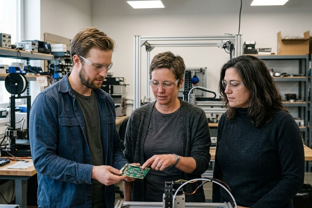
This site is maintained by a technical team that works across printed electronics research, equipment understanding, application development, and manufacturing translation. The mix matters. A process engineer notices different problems than a materials researcher. A product designer asks different questions than a production technician. Good content needs all of those pressures in the room.
Our approach starts with prior work: known inkjet printing behavior, established conductive materials practice, and the lessons already learned in flexible electronics. The gap we try to address is the space between general explanation and usable implementation detail. Many readers do not need another broad definition of printed electronics. They need to know what to check before committing to an ink, a substrate, a curing method, or a machine configuration.
That is why our writing favors comparisons, process notes, and application-specific framing. When we describe a method, we explain where it fits. When we discuss equipment, we connect hardware choices to print quality and repeatability. When we cover research, we try to show what the work suggests and what still needs validation for a specific use case.
If you are evaluating conductive inkjet for a product, a prototype, or a manufacturing study, this site is meant to be a steady reference. Start with the section closest to your decision, then move outward. The best printed electronics work rarely comes from one perfect setting. It comes from aligning material, pattern, substrate, equipment, and test method until the circuit behaves the way the application needs it to behave.