Applications
Moulded Electronic Components: Carclo plc Case Study
ESC closes search
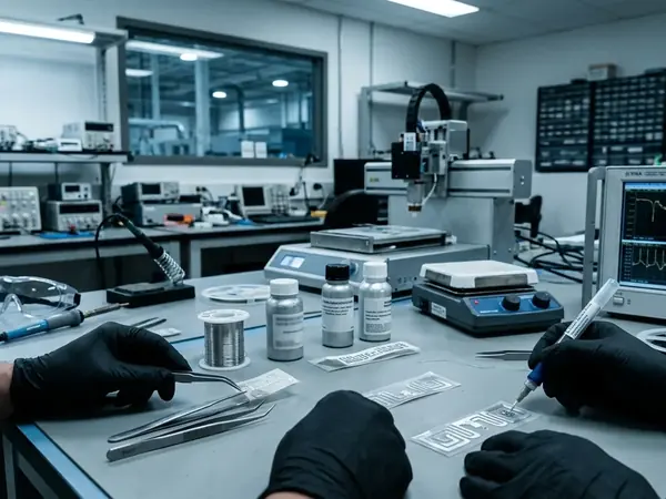
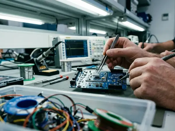
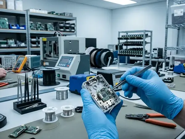
Print2Chip applications sit at the point where semiconductor packaging, printed electronics, and hardware prototyping stop being separate conversations. This category examines how conductive inkjet processes enable touch surfaces, sensors, RFID structures, flexible circuits, and advanced package interconnects without defaulting to subtractive board workflows. The strongest examples are practical: additive antenna production, direct-to-chip deposition trials, and integrations that must survive real curing, adhesion, and placement constraints.
Readers working in this area usually care less about whether printing can draw a conductive line and more about whether that line remains useful after encapsulation, thermal exposure, handling, and connection to existing components. That is why the category leans toward case-based coverage: droplet placement on dielectrics, ink behavior near pads, heterogeneous integration decisions, and the tradeoffs that appear before a prototype becomes a repeatable process. For packaging engineers and printed-electronics researchers, the valuable detail is often mundane: surface preparation, cure window, line edge control, and how the printed feature meets a plated contact or mounted part.
Print-to-chip methods do not replace silicon wafer fabrication, and conductive inks should not be treated as bulk copper by another name. The useful question is narrower and more demanding: where can controlled deposition reduce packaging complexity, shorten iteration cycles, or make a form factor possible that conventional routing would make awkward. Those details decide whether an application belongs in the lab or on the process sheet.