Applications
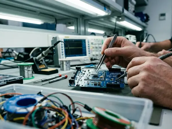
Moulded Electronic Components: Carclo plc Case Study
ESC closes search
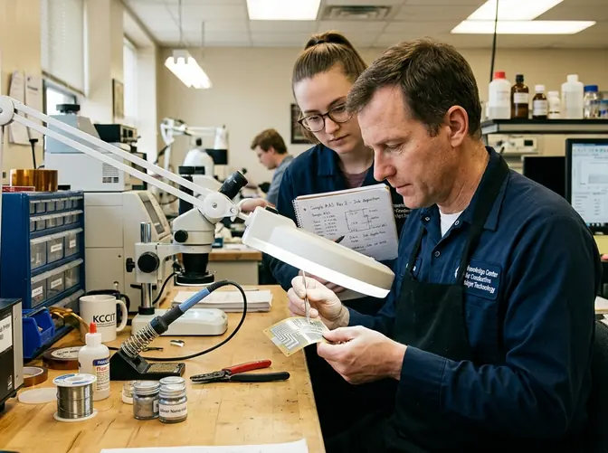
Conductive inkjet work rarely fails in the headline concept. It fails in the details: a nozzle that drifts after lunch, a silver trace that measures well before forming, a substrate coating that looks identical until the first adhesion pull.
This knowledge center is built for engineers, researchers, and manufacturers who need those details in plain technical language. The focus is conductive inkjet technology for printed electronics, including MetalJet deposition, Liquid Wiring methods, Print2Chip integration, flexible circuits, RFID antennas, sensors, and transparent conductive film concepts.
The working assumption is simple: useful printed electronics guidance should connect ink behavior, jetting conditions, substrate preparation, curing, and downstream integration. Treating any one of those as a standalone topic makes the process look cleaner than it is on the bench.
Because printed electronics performance depends heavily on ink chemistry, substrate stack, and post-cure sequence, conclusions here stay tied to the process conditions being discussed rather than presented as universal recipes.
A good conductive inkjet note should help someone make a decision before material is wasted. That might mean choosing between a finer feature and a wider process window, setting up a waveform trial, or deciding whether a printed antenna belongs on a polymer film, moulded component, or label stock.
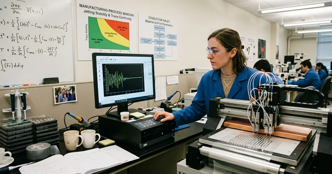
Coverage includes functional ink behavior, drop formation, satellite control, nozzle health, and the practical limits of fine-line deposition.
Surface energy, coatings, roughness, and thermal tolerance often decide whether a good print becomes a usable circuit.
Electrical continuity is only the starting point. We look at post-processing, forming, encapsulation, device assembly, and inspection.
Testing confirmed one recurring lesson in conductive inkjet development: waveform setup, ink condition, and substrate preparation have to be read together. A stable drop on glass does not guarantee the same behavior on a coated polymer web or a shaped moulding.
When comparing printed electronics processes, the lowest-resistance sample is not always the best manufacturing route. Repeatability, alignment tolerance, handling damage, and rework access can matter more once the process leaves the lab.
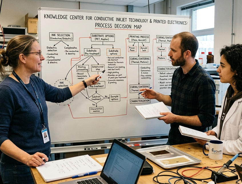
The site is organised around the way engineers normally approach a printed electronics project: understand the technology, select equipment, match the application, define the manufacturing route, review research, then keep the reference material close during build-out.
Core conductive inkjet processes, MetalJet deposition concepts, and the physics behind stable printed conductors.
View Technology
MetalJet systems, deposition hardware, inspection tools, and the production details that affect uptime.
View Equipment
Touch surfaces, sensors, UHF RFID antennas, transparent films, and flexible circuit use cases.
View Applications
Production methods, Liquid Wiring techniques, process windows, and scale-up constraints.
View Manufacturing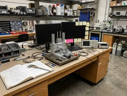
Applied studies, prototyping methods, and early-stage device translation for conductive inkjet processes.
View Research
Technical references, terminology, case context, and industry notes for printed electronics teams.
View ResourcesMost printed electronics projects begin with a narrow demonstration: a conductive line, a simple antenna, a touch electrode, or a sensor trace. The hard part is turning that demonstration into a repeatable route without losing the electrical or mechanical behavior that made it interesting.
Prior work in the field has shown that additive deposition can reduce material waste and open design options that subtractive etching cannot match. The gap appears when teams move from a flat coupon to a real device stack. Registration, surface contamination, thermal budget, and contact resistance become part of the same problem.
Our approach is to discuss the route as a chain, not a single print step. For example, a UHF RFID antenna is not just a pattern geometry. It also depends on ink loading, film handling, sintering profile, chip attach method, and the environment where the tag will be read. The same thinking applies to moulded electronic components, where forming and overmoulding can expose weaknesses that looked harmless on a flat test piece.
For device examples, start with the UHF RFID printed antennas case study or the moulded electronic components case study. Both topics show why geometry and production handling need to be considered together.
For process fundamentals, the conductive inkjet printing methodology overview is the better entry point. It sets up the vocabulary used across the technology and manufacturing sections.
conductiveinkjet is written for readers who notice when a process description skips the awkward step. The editorial group combines manufacturing applications, functional ink research, process development, technical editing, technology strategy, and industry analysis.
Manufacturing Applications Engineer focused on scale-up of conductive inkjet processes for printed electronic devices.
Principal Research Scientist, Functional Inks, covering first-principles modelling, jetting stability, and electrical percolation.
Senior Process Development Engineer specialising in method development, validation, and process windows for conductive inkjet manufacturing.
Technical Editor, Printed Electronics, translating foundational physics into clear technical interpretation for engineering readers.
Senior Technology Strategist covering printed electronics platforms, integration routes, and market readiness.
Senior Industry Analyst, Printed Electronics, focused on manufacturing case studies, market translation, and device commercialisation.
If a conductive inkjet project is moving from sample prints to a device trial, the best time to check the process assumptions is before the purchase order for tooling, fixtures, or pilot material goes out.
Start with the process fundamentals, then move into application and manufacturing guidance once the substrate, ink family, feature size, and post-processing route are known. That order saves time because it keeps the discussion close to the constraints that actually govern printed electronic devices.