Manufacturing Challenges for UHF RFID Antennas
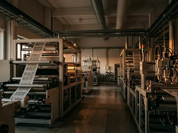
Subtractive copper etching remains the default route for UHF RFID antenna production, yet the process carries structural inefficiencies that compound at volume. The engineering team mapped the chemical degradation of the ferric chloride baths across continuous production shifts, and the pattern that emerged was instructive: undercut variations tracked directly to etchant saturation rather than to mask alignment or exposure timing. As the bath chemistry drifted, so did trace geometry, and with it the impedance behaviour of the finished antenna.
This matters because UHF antennas tolerate very little dimensional slack. A trace edge that wanders by tens of microns shifts the resonant point and narrows the usable read window.
The waste profile is the second concern. Subtractive workflows start with a fully metallised laminate and remove the majority of that copper to leave the conductive pattern behind. Most of the deposited metal never reaches the final device. For a product line measured in millions of units, that discarded copper represents both a recurring material cost and a downstream effluent management burden.
Design freedom suffers as well. Each new antenna geometry demands a fresh photomask, which slows iteration and discourages the kind of rapid layout tuning that frequency-specific applications often require. These constraints together explain why printed electronics teams have looked steadily toward scalable additive alternatives.
Adopting the Additive Process with CIT Printed Antennas
The shift to an additive route did not begin with inkjet. Engineers first evaluated rotary screen printing, but the paste viscosity limited achievable resolution below what UHF geometries demand. Screen printing suited coarse conductive patterns; it could not hold the fine trace edges these antennas needed.
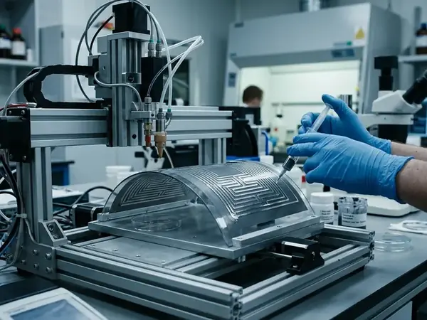
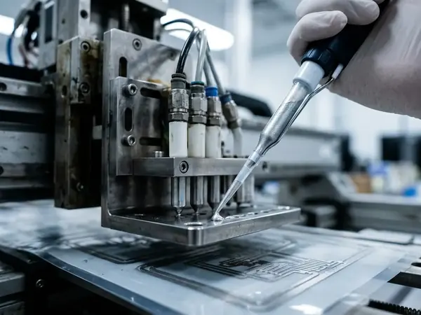
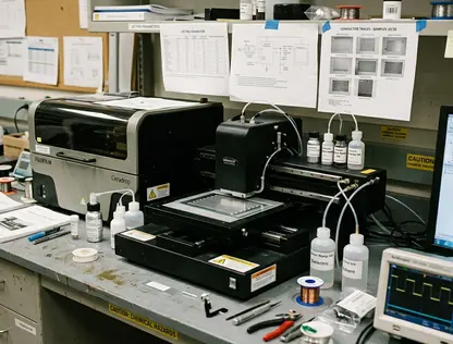
Piezoelectric inkjet deposition of catalytic inks proved the more workable path. The process lays down a catalyst pattern through a digital printhead, then grows the conductor through electroless copper plating on that seeded geometry. Copper remains the primary metal in the workflow, which keeps the conductivity profile familiar to engineers accustomed to etched copper antennas.
According to measurements taken during process calibration, the piezoelectric drop volumes were held between roughly 2.5 and 4.0 picoliters, with curing maintained at about 145°C for 12 to 15 minutes. Those parameters define the deposition window for the CIT Printed Antennas line, where digital patterning replaces the mask entirely.
The integration point worth noting is that the catalytic ink and the plating step form a single coordinated sequence. The printer defines where copper will appear; the bath defines how thick it grows. This separation of patterning from metallisation is what gives the additive route its flexibility.
Additive Versus Subtractive Etch Approaches
The clearest way to understand the two routes is to set their process flows side by side.
{{TABLE}}
The subtractive flow front-loads its complexity into photolithography and masking, then removes bulk foil to reveal the pattern. The additive flow inverts this: direct digital inkjet deposition defines the geometry, and electroless copper growth on the catalyst builds the conductor only where it belongs.
Flexibility and precision
Digital patterning carries an obvious advantage for iteration. A layout change is a file change, not a new physical mask. For a facility running several antenna variants across UHF sub-bands, that responsiveness shortens the gap between design revision and printed sample.
Precision follows from the same mechanism. The drop volume window cited earlier governs feature resolution directly, and tuning it adjusts trace definition without retooling.
Material efficiency
Because copper grows only on the catalysed pattern, the additive route deposits metal where the design calls for it rather than across the whole substrate. The contrast with bulk foil reduction is stark. There is no full-sheet metallisation to strip away, which trims both raw copper consumption and the volume of spent etchant entering the waste stream.
During production reviews, facility managers audited the floor layout and decided to physically bypass the photolithography zones. Removing that stage reduced the footprint of the antenna manufacturing cell, a practical consequence of the additive flow that does not show up in a process diagram.
Performance Outcomes in UHF RFID Applications
Validation determines whether a manufacturing decision survives contact with a real device. The testing committee declined to rely on simulated impedance matching and instead mandated physical anechoic chamber sweeps across the global UHF band. The reasoning was specific: skin-effect behaviour in electroless copper needed empirical confirmation rather than modelled assumption.
Recorded results show read ranges spanning roughly 8.2 to 8.6 meters, with cured trace sheet resistance stabilised at about 0.04 ohms per square. Those figures place the additive antennas within the operating envelope expected of conventional etched parts, which was the threshold the committee set for adoption.
The choice to deploy additive antennas for these particular use cases rested on more than electrical parity. The combination of low waste, mask-free iteration, and a smaller production footprint tipped the decision where design variants needed frequent revision. For high-mix, frequency-specific work, the additive route earned its place on measured performance rather than projected benefit.
One mechanical constraint shapes deployment. The additive copper layer can suffer antenna detuning from micro-cracking when bent below a 15-millimeter radius on rigid PET. Applications that demand tighter flexing require substrate and geometry choices that account for this limit. Engineers working to formal performance criteria may also consult the IEEE standards on RFID antenna performance when defining acceptance thresholds.
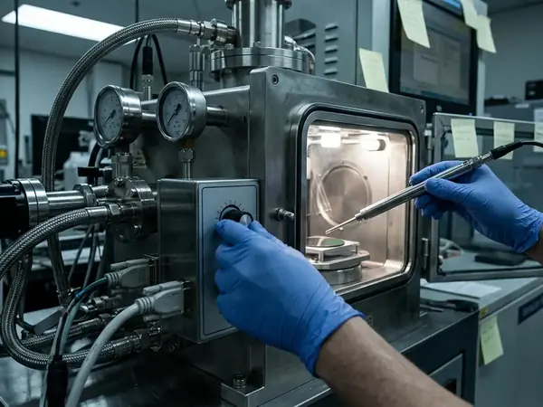
The plating thickness is not a free parameter. The required electroless copper depth varies strictly with the target frequency's skin depth, so lower-frequency applications demand longer bath dwell times to reach the conductivity the band requires.
Summary and Implementation Considerations
For engineers weighing the additive route, the core advantages cluster around three points. Material is deposited rather than removed, which cuts copper waste and effluent load. Patterning is digital, which collapses the iteration cycle for new geometries. And the performance measured in the anechoic chamber landed within the range expected of etched parts, so the gain in efficiency did not cost read range.
The implementation guidelines for this work were drafted by cross-referencing the thermal deformation thresholds of various PET substrates against the electroless copper plating temperatures the process requires. That cross-reference is the practical heart of substrate selection.
Where the approach reaches its edge
One catch deserves emphasis. Catalytic ink adhesion degrades rapidly on untreated low-surface-energy plastics such as PTFE, which forces an inline corona treatment step before deposition. Teams targeting those substrates should budget for that stage from the outset.
A note on scope: these findings come from a defined set of UHF antenna builds on PET, validated against a specific acceptance threshold. They describe what this configuration achieved rather than a universal result for every additive antenna programme. The skin-depth dependence and the bend-radius limit both point to where reproduction would require fresh characterisation against the target application.
Summary: additive CIT antenna production offers genuine material and iteration gains for UHF work, provided substrate energy, plating thickness, and mechanical flex are characterised against the intended band and form factor before committing to volume.