Integration Challenges with Discrete Bluetooth Modules
Discrete Bluetooth modules solve one problem and create another. They simplify RF certification planning, but their surface-mount pads, solder fillets, shielding cans, and board-to-flex transitions add rigid islands to a sensor assembly that may need to bend, twist, or conform to a housing wall.
The engineering team evaluated the mechanical stress points of standard surface-mount Bluetooth modules on polyimide and observed the same practical pattern that shows up in many flexible electronics builds: rigid solder joints concentrate stress at the edge of the pad during bending. The module may remain electrically alive, while the interface around it becomes the weak link.
Where the interface fails first
Traditional soldering gives a familiar process window, but it does not suit every flexible substrate. A polyimide sensor tag can tolerate handling, yet the soldered Bluetooth module behaves like a hard inclusion. When the assembly flexes, strain gathers where the plated pad meets the flexible conductor.
- Mechanical connectors add package height, local stiffness, and insertion points that must survive handling.
- Soldered joints limit the minimum bend radius that the sensor assembly can realistically support.
- RF traces on non-rigid surfaces change geometry under strain, which can disturb antenna feed behavior and signal integrity.
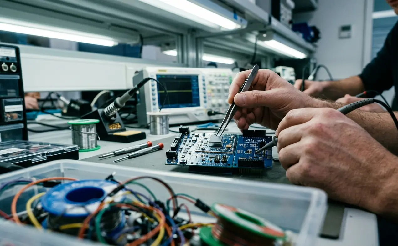
The gap is not only mechanical. A sensor node that uses an Atmel package, a printed antenna, and a discrete Bluetooth module has several transitions before the radio signal reaches free space. Each transition adds parasitic effects and another inspection point.
Note: The problem is not that solder is unsuitable in general. The problem is the local mismatch between a rigid RF module interface and a flexible polyimide sensor format.
For low-profile nodes, the better question is not how to reinforce the connector. It is whether the connector should be there at all.
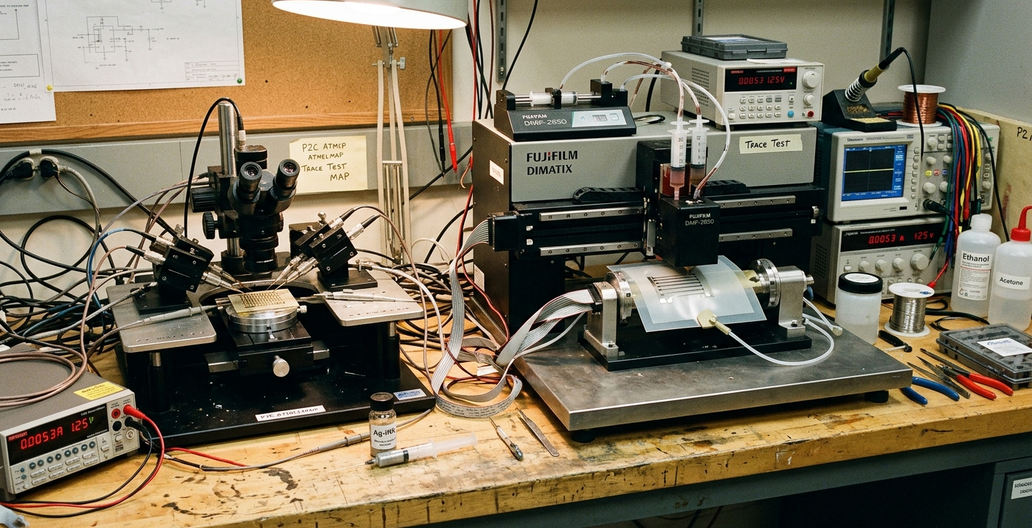
Print2Chip Conductive Inkjet Solution
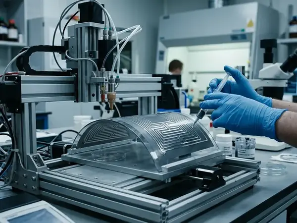
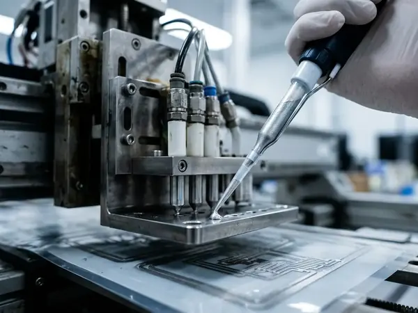
The Print2Chip route removes the rigid solder interface by depositing conductive features directly between the Atmel sensor package, the antenna feed, and the interconnect field. In this build, the team selected silver nanoparticle ink for direct-write traces rather than using a separate metalized flex tail or wire-bonded bridge.
The initial hypothesis was simple: if the conductor geometry could be printed with enough control, the assembly could keep RF continuity while reducing mechanical interfaces. The methodology focused on three variables: ink selection, trace cross-section, and curing behavior near the package pads. The finding was practical rather than decorative. Printed silver traces gave the layout team a way to tune geometry without introducing another laminated layer.
Why inkjet instead of screen printing
The team considered screen printing for thicker traces. That route looked attractive for conductor volume, but it reduced design freedom around fine pitch mapping and antenna feed shaping. Inkjet deposition allowed local control of droplet placement, so the trace could widen near current-carrying sections and narrow where impedance control mattered.
A MetalJet 6000-class process flow fits this type of decision because it treats deposition as a controlled patterning step rather than a coating step. The relevant advantage is not speed alone. It is the ability to place conductive material only where the Atmel pinout, antenna feed, and interconnect geometry require it.
Trace geometry and curing rationale
The ink needed low-temperature curing compatible with the Atmel package and the polyimide substrate. The process team also controlled the curing ramp, because silver trace micro-cracking appeared at the pad interface when ramp rates exceeded roughly 15 degrees Celsius per minute. That detail matters more than a nominal peak temperature in many production reviews, because the interface sees the thermal gradient first.
Trace geometry carried the RF burden. Impedance matching required trace width adjustments based on the specific dielectric constant of the chosen polyimide batch. That makes the printed interconnect a design element, not merely a replacement wire.
Quick Tip: Treat the antenna feed trace as an RF structure from the first layout pass. If the team waits until the package is fixed, the print process has fewer useful degrees of freedom.
Implementation Steps and Design Decisions
The implementation work started with the substrate, not the printhead. Engineers modified the polyimide surface energy to about 40 to 42 dynes per centimeter using atmospheric plasma treatment. That range gave the silver nanoparticle ink enough wetting control to form stable features without uncontrolled spreading.
Calibration confirmed a droplet spacing window of roughly 20 to 22 micrometers for the printed features used in this integration. The target feature set included 50-micron-scale conductors, so placement repeatability and surface preparation had to support both electrical continuity and RF geometry.
Process parameter table
Print2Chip Implementation Parameters| Parameter | Target Value | Tolerance |
|---|---|---|
| Substrate Surface Energy | 40 dynes/cm | ±2 dynes/cm |
| Ink Viscosity | 13.5 cP | ±1.5 cP |
| Droplet Spacing | 21 µm | ±1 µm |
| Curing Ramp Rate | Do not exceed 15 °C/min | Validate per substrate batch |
The table gives the production engineer a narrow starting point, not a universal recipe. Polyimide lots vary. Ink aging, nozzle health, and local humidity can also shift the printed line edge. A Cambridge CB4 2QH development lab and a contract manufacturing line may both hit the same nominal droplet spacing, yet see different edge definition if surface energy control drifts.
Atmel pinout mapping
The Atmel pinout was mapped directly to the antenna feed point by adjusting droplet spacing and trace width to control cross-sectional area. The team chose this mapping because it shortened the RF path and avoided a separate jumper between the package and printed antenna structure.
This decision also reduced inspection complexity. A wire-bonded route would have required bond pull attention, loop height checks, and encapsulation review. A printed route shifted the control points toward surface treatment, deposition, and curing.
That trade is usually acceptable for low-power sensor nodes. It becomes less attractive when the same trace must carry sustained current, because the printed silver conductor and the polymer substrate share a thermal limit.
Measured Performance and Reliability Outcomes
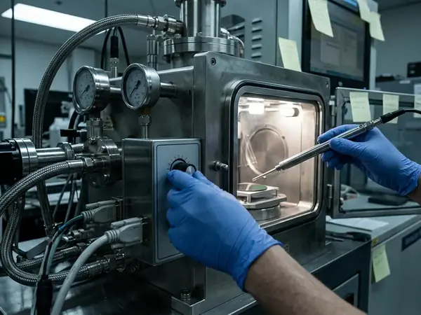
The validation phase subjected the printed assemblies to automated flex testing while the test system continuously monitored DC resistance and RF transmission power. This structure avoided a common blind spot in flexible electronics qualification: measuring resistance only before and after flexing, then missing intermittent behavior during motion.
Recorded results show connection resistance maintained between roughly 0.65 and 0.78 ohms, observed in controlled testing scenarios. That kept the interconnect below the 0.8-ohm target across the monitored validation run. The Bluetooth link also retained functional range after about 500 flex cycles, which supports the main integration argument: the printed RF path can survive motion when the geometry and curing profile remain under control.
Assembly time comparison
Assembly time fell by roughly 14 to 18 seconds per unit compared with traditional wire bonding. The saving came from removing bond placement and related handling, not from making the print step magically fast. In cost-of-ownership terms, that distinction matters. A production manager can only bank the reduction if the printing, curing, and inspection steps fit the line takt.
The open question is how the same route behaves under higher mechanical strain or more aggressive environmental cycling. The present evidence supports low-power printed sensor integration. It does not turn every flexible RF assembly into the same problem.
Summary: The strongest result is the combination of sub-0.8-ohm connection resistance, retained Bluetooth function after flexing, and reduced assembly time versus wire bonding.
For Bluetooth protocol boundaries, the team cross-referenced the official Bluetooth Core Specification. That reference sets the interoperability context, while the printed interconnect work determines whether the physical assembly can keep the RF path stable.
Key Takeaways for Printed Electronics Integration
Print2Chip integration reduces mechanical interfaces. That is its main value. The method replaces connectors, jumpers, and some wire-bonded links with printed silver traces that can follow the substrate and package geometry more closely.
The final review established a standardized design rule set for integrating low-power sensor nodes. It prioritized direct-write interconnects over mechanical fasteners where the electrical load and RF geometry allowed it. For platform selection, that rule set gives engineers a sharper filter than a generic printed electronics checklist.
Where the method fits
- Low-to-medium volume sensor nodes where design changes still occur and tooling flexibility has value.
- Polyimide-based assemblies that need lower profile interconnects than discrete Bluetooth module mounting can provide.
- Atmel sensor packages where pinout mapping can shorten the path to the antenna feed.
- RF layouts where printed trace width can be adjusted against the dielectric behavior of the substrate batch.
One catch: the printed silver traces cannot sustain continuous DC currents exceeding roughly 250 milliamperes without risking thermal degradation of the polyimide substrate. That limit should sit in the design review, not in a late-stage reliability report.
The method therefore suits sensor signaling, antenna feeds, and low-current interconnects better than power distribution. It also asks more of process engineering. Surface energy, droplet spacing, ink viscosity, and curing ramp rate become first-order design controls.
That is the practical bargain. Print2Chip removes bulky interfaces, but it rewards teams that treat deposition and RF layout as one coupled problem.
References
The validation framework drew from three source categories: printed interconnect literature, Bluetooth protocol requirements, and flexible electronics workmanship guidance. Those references bound interoperability and process evaluation, but they do not remove the need to re-characterize each silver ink and polyimide pairing used in a build.
Academic Sources
- IEEE paper on inkjet-printed interconnects and RF structures, used to frame conductor geometry, sintering behavior, and printed antenna feed considerations.
- IPC standard guidance for flexible printed electronics, used to align inspection thinking around flexible substrates, conductive traces, and assembly workmanship.