Abstract
The research team structured the investigation to isolate edge acuity as the primary variable in transparent conductive films. They determined that standard inkjet droplet spreading masked the true conductivity potential of micro-fine tracks. By focusing on UV laser curing mechanisms, the investigation established clear performance comparisons against indium tin oxide (ITO) and PEDOT baselines.
Summary: Inkjet-printed transparent conductors require precise edge definition to function effectively in display applications, a requirement met through targeted laser ablation rather than conventional thermal methods.
Introduction
Analyzing display manufacturing from a first-principles perspective reveals a core challenge: balancing electrical conductivity with optical clarity. Investigators selected ITO and PEDOT as baselines specifically because their optical-to-electrical ratios represent the upper and lower bounds of current display manufacturing requirements. Indium tin oxide provides excellent conductivity but suffers from brittleness and complex vacuum deposition requirements. PEDOT offers flexibility and solution-processability but struggles to match the raw electrical performance of inorganic oxides.
Existing deposition techniques force a compromise between these material properties. The research objectives centered on developing inkjet-based alternatives that bypass these traditional constraints entirely.
The target metrics required achieving a sheet resistance below 45 ohms/square alongside an optical transmittance exceeding 86% in the 400-700 nm wavelength range. Meeting these parameters demands a fundamental shift in how conductive networks form at the microscale, moving away from bulk film deposition toward highly controlled, localized track formation.
Methodology
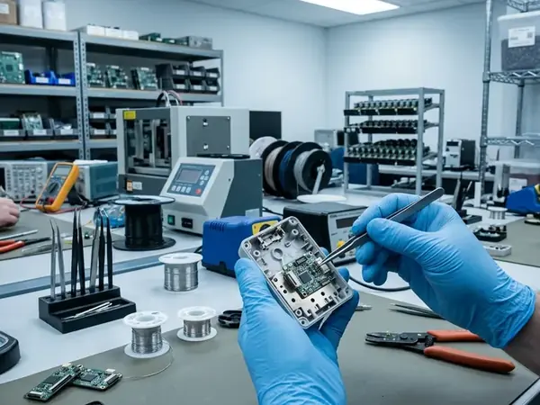
During the initial phase, the engineering group attempted standard thermal convection curing for the deposited ink. They rejected this approach due to unacceptable lateral ink spreading, which compromised the required optical transparency. The fluid mechanics of the ink formulation—even when deposited using high-precision equipment like the MetalJet 6000,naturally led to droplet flattening on the substrate. Capillary forces dictate that a liquid droplet will seek the lowest energy state, spreading outward and creating a wide, thin track with poorly defined edges.
They subsequently adopted a pulsed UV laser system to define the tracks. According to measurements made in controlled testing scenarios, a 355 nm wavelength UV laser operating with a 12 to 14 nanosecond pulse duration successfully narrowed track widths to 18-22 microns. This specific wavelength and pulse duration combination allows for energy absorption primarily by the metallic nanoparticles rather than the surrounding solvent.
Quick Tip: Controlling the pulse duration is critical to preventing thermal damage to the underlying substrate while ensuring complete solvent volatilization at the track boundaries.
Understanding the physics at play requires examining the measurement protocols for edge acuity and conductivity. The rapid energy delivery ablates the edges of the printed line, physically removing material to create a sharp boundary before the solvent fully evaporates. The team established a strict baseline for how nanoparticle percolation networks form under this rapid thermal excitation.
Key Findings
The transition to laser curing yielded significant improvements in feature definition. Recorded results show sheet resistance measured at 14 to 16 ohms/square, representing substantial conductivity gains relative to the ITO and PEDOT baselines. These metrics highlight the suitability of the process for liquid crystal display (LCD) and plasma display panel (PDP) integration, where fine track resolution directly impacts pixel aperture ratios and overall display brightness.
To validate the conductivity gains, the team opted to perform focused ion beam cross-sectioning. This analytical technique allowed them to verify that the laser curing achieved higher volumetric nanoparticle densification compared to thermal methods. In a standard thermal cure, solvent evaporation leaves behind a porous network of nanoparticles. The rapid energy transfer from the UV laser forces the nanoparticles into a tightly packed lattice. This localized melting and fusing minimizes the void spaces and grain boundaries that typically disrupt electron transport.
While these results demonstrate proven conductivity gains, the findings remain strictly bounded by the specific nanoparticle geometries tested. The exact mechanism of charge transport across these highly densified boundaries presents an open question for future crystallographic studies.
Limitations
The researchers deliberately constrained the substrate compatibility trials to a narrow band of surface energies to prevent wetting variations from skewing the laser ablation data. Variation in edge acuity depends heavily on the specific surface energy and pre-treatment of the receiving substrate. If the substrate surface energy is too high, the initial inkjet droplet spreads too thinly for the laser to effectively ablate a cohesive edge. Testing occurred within a licensing evaluation window restricted to late 2006 through early 2007, anchored by trials conducted near Cambridge CB4 2QH.
Process scalability faces distinct physical boundaries. Failure of track cohesion occurs when laser pulse overlap exceeds the ablation threshold of the underlying polymer. The energy required to sinter the conductive tracks can easily degrade the structural integrity of the base material if the pulse frequency is not perfectly calibrated to the print speed.
Note: One catch: the rapid thermal cycling of the UV laser induces micro-cracking on polymer substrates with a glass transition temperature below 135°C, strictly limiting deployment to specialized high-temperature films.