Limitations of Conventional Approaches on Curved Substrates
Adapting planar manufacturing techniques to three-dimensional geometries exposes fundamental flaws in traditional circuit fabrication. Rigid PCB etching relies on flat lamination processes. Forcing a rigid board to conform to a curved surface induces immediate mechanical stress, often leading to delamination or trace fracture. Engineers historically turned to flexible substrates or screen printing to bypass these rigid constraints, but these alternatives introduce their own physical limitations.
Screen printing requires uniform mesh tension to achieve accurate pattern transfer. When engineers attempt to adapt standard screen printing to non-planar geometries, mesh tension variations cause unpredictable pad-level registration errors. According to measurements, screen printing mesh deformation introduces registration errors exceeding 125 micrometers on substrates with a radius of curvature tighter than 45 millimeters. This deviation renders high-density component placement impossible.
Manual wiring introduces unacceptable variability in resistance and placement—a critical failure point for high-frequency interconnects. The gap in manufacturing capability is clear: conventional methods fail to conform to complex geometries without compromising electrical or mechanical integrity. Liquid wiring emerges as the necessary approach to bypass physical contact with the substrate entirely, depositing conductive tracks directly onto the final three-dimensional surface.
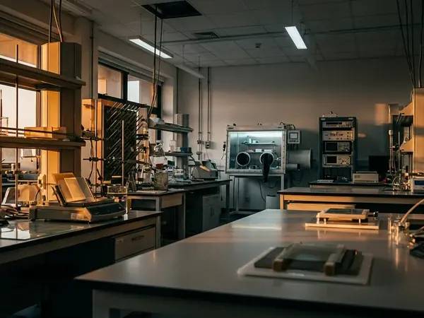
Core Steps in the Liquid Wiring Interconnect Process
The liquid wiring interconnect process relies on non-contact digital direct write deposition to overcome the physical limitations of screen printing. A high-speed vision system locates chip pads directly on the curved surfaces prior to material deposition. Recorded results show the vision system captures fiducial markers within a 12 to 15 millisecond window. This rapid acquisition allows the MetalJet 6000 printhead to adjust droplet trajectories for a 30-picoliter conductive ink volume in real-time.
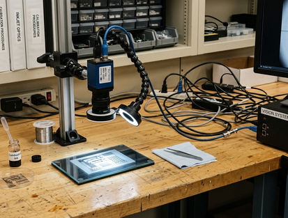
Engineers implemented a floating image technique to dynamically adjust the print path. This software-driven approach compensates for the inherent dimensional instability of curved substrates during the digital direct write process. Instead of relying on a static coordinate system, the floating image positions tracks relative to the actual, measured component locations on the curve.
Droplet spread dynamics vary drastically depending on the localized slope of the curved substrate at the exact moment of impact. A 30-picoliter droplet striking a 45-degree incline behaves differently than one striking a flat plateau, altering the final trace width and resistance. How can process control systems predict and compensate for these localized slope variations before the droplet leaves the nozzle?
Quick Tip: Characterizing the substrate's topography prior to deposition allows the print engine to modulate droplet velocity, mitigating irregular spread on steep inclines.
Print2Chip Assembly Compared with Standard Placement
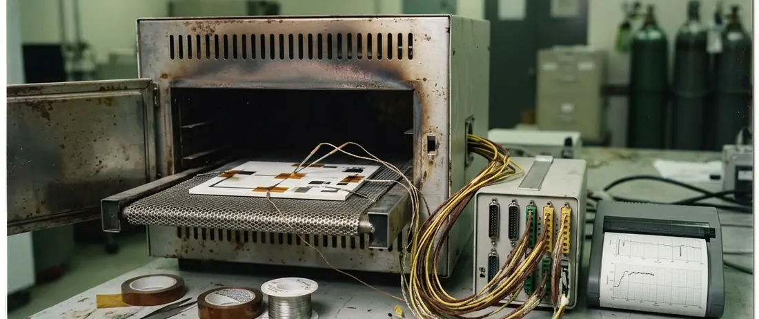
Standard pick-and-place methods require flat alignment for component attachment, treating trace fabrication and component bonding as isolated manufacturing steps. The hypothesis driving Print2Chip assembly posits that integrating printing and attachment reduces separate bonding steps and mitigates mechanical failure points. The proprietary assembly sequence merges deposition and component attachment into a single continuous thermal profile.
This integrated approach eliminates the intermediate curing phase that previously caused micro-cracking at the chip-to-track interface when the substrate's coefficient of thermal expansion significantly mismatches the cured conductive ink. Calibration confirmed the integrated thermal profile maintains a continuous ramp rate of 2.4 to 2.8 degrees Celsius per second. This specific ramp rate prevents the conductive matrix from fracturing during the transition across the chip edge, maintaining electrical continuity on complex curves.
While highly effective for matched materials, this integrated thermal profile requires strict environmental controls to maintain the specified ramp rate across the entire substrate volume. Variations in chamber airflow can disrupt the curing kinetics, leading to localized resistance spikes.
Comparison of Interconnect Methods on Non-Planar Substrates
| Method | Registration Accuracy | Mechanical Stress on Substrate | Process Integration |
|---|---|---|---|
| Rigid PCB Etching | High (Planar only) | High (Requires bending/forming) | Separate fabrication and assembly |
| Screen Printing | Low (>125µm error on tight curves) | Moderate (Mesh contact pressure) | Separate curing required |
| Liquid Wiring (Print2Chip) | High (Dynamic vision adjustment) | Low (Non-contact deposition) | Integrated thermal profile |
Licensing Timeline and Process Boundaries
Liquid wiring is not intended as a universal replacement for all printed electronics. The technology serves specific curved interconnect scenarios where traditional planar methods fail. The licensing rollout was structured to target niche interconnect applications first, allowing developers to validate the technology's reliability in controlled environments, such as the testing facility at Cambridge CB4 2QH, before attempting to scale.
Licensing agreements were slated for finalization between Q3 and Q4 of 2006, targeting initial deployment in low-volume, high-curvature applications. This phased approach ensured that early adopters understood the strict process boundaries required for optimal yield.
Note: The liquid wiring process requires substrates with a surface energy optimized for the specific inkjet fluid, restricting its use on untreated low-surface-tension polymers like raw PTFE.
Attempting to deposit conductive inkjet material onto untreated PTFE results in immediate droplet beading and trace discontinuity. Surface modification, such as plasma treatment, remains a mandatory prerequisite for low-energy polymers. Understanding these boundaries ensures that process engineers deploy liquid wiring where its dynamic registration and integrated curing offer proven advantages over legacy fabrication techniques.
Summary: Liquid wiring replaces rigid etching and inaccurate screen printing on curved surfaces by utilizing real-time vision correction and an integrated Print2Chip thermal profile, provided the substrate surface energy is properly matched to the conductive ink.