Conductive inkjet printing is easiest to understand when you separate the job into two parts: print a precise polymer template, then grow metal only where that template sits. The inkjet head does not usually print a thick copper conductor directly. It prints the geometry that tells the later copper deposition step where to build the interconnect.
That distinction matters. It shifts the hard problem from forcing metallic ink through a nozzle to controlling wetting, curing, and surface chemistry with enough discipline that the metallization step stays selective.
Contents
- Materials and Hardware Components
- Deposition Protocol Using Piezo Heads
- Electroless Metallization Step
- Comparison to Photolithography and Sputtering
- MetalJet 6000 Production Platform
Materials and Hardware Components
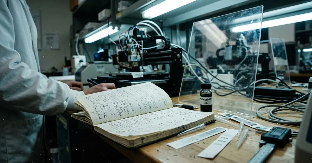
The core stack is deliberately modest: a UV-curable template ink, piezo industrial print heads, and copper for secondary deposition. In practice, the quality of the final conductor depends less on any one material than on how these three components behave as a coupled process.
Template ink and print-head selection
The UV-curable ink serves as the printed template material. It defines the future copper path, fixes the line geometry after cure, and presents the surface chemistry needed for selective metallization. I tend to describe it as a functional resist rather than a conventional conductive ink, because its first duty is spatial control.
Engineers selected piezo industrial print heads over thermal inkjet alternatives because thermal stress from thermal heads degraded the UV-curable polymer chains before deposition. That is not a small materials detail. If the polymer changes before it reaches the substrate, the cured template no longer behaves like the template qualified during process development.
Piezo heads avoid that thermal load by using actuator deformation to eject the droplet. The operating window still needs discipline: the heads run at frequencies between roughly 20 kHz and 35 kHz, while the UV-curable ink viscosity is maintained between about 10 and 15 centipoise at 45°C.
Copper as the conductive phase
Copper is the standard metal for the secondary deposition stage because it forms the actual conductive interconnect after the polymer template has cured. The printed ink defines location; the copper supplies current-carrying capacity.
Summary: Conductive inkjet printing, in this process family, is not simply “printing metal.” It is template printing followed by selective copper growth.
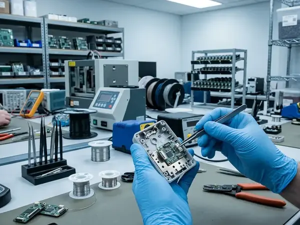
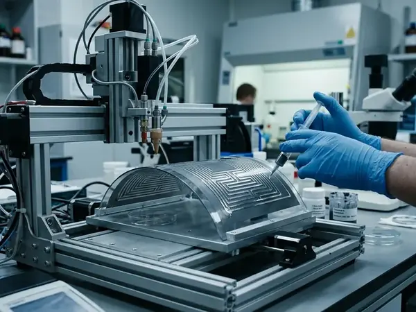
Deposition Protocol Using Piezo Heads
The deposition protocol starts with a direct-write pass using MetalJet-UV inks. The goal is not maximum ink delivery. The goal is a stable droplet that lands where intended, spreads by a controlled amount, and cures before surface flow can blur the feature.
Waveform calibration and droplet control
Calibration confirmed that the piezo actuator waveform must match the acoustic impedance of the MetalJet-UV inks to produce satellite-free drop formation. This is the point where the physics becomes visible on the substrate. An uncalibrated waveform can create small satellite droplets around the main drop, and those stray deposits can become short-circuit sites after copper growth.
Drop volumes are calibrated to a strict 2 to 4 picoliter range. Small changes matter because the droplet volume controls line width, edge definition, and local template thickness. On a dense interconnect pattern, a few misplaced droplets can close a designed gap.
Substrate preparation and UV pinning
Substrate preparation sets the wetting boundary before the first drop lands. The surface must accept the printed template without encouraging uncontrolled spread. That usually means treating cleaning, surface energy, and handling as part of deposition rather than as housekeeping.
After impact, UV pinning occurs within roughly 50 to 150 milliseconds. This short interval limits droplet movement while still allowing enough leveling for a coherent line. If the cure arrives too late, capillary flow can round corners and widen traces. If it arrives too aggressively, the line can freeze before neighbouring droplets merge cleanly.
- Prepare the substrate so the template ink wets predictably.
- Set ink temperature and viscosity inside the qualified range.
- Calibrate the piezo waveform for the MetalJet-UV ink batch.
- Print the direct-write pattern with controlled drop spacing.
- Pin the deposited ink with UV exposure within the process window.
Quick Tip: When a printed feature looks correct before metallization but shorts after copper growth, inspect the droplet field rather than only the plating bath. Satellite droplet formation is often easier to miss than a visibly overgrown trace.
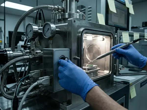
Electroless Metallization Step
Once the UV template has cured, the process changes character. Printing has done its spatial work. The electroless copper bath now has to grow metal selectively on that printed chemistry without plating the bare substrate.
Bath chemistry, temperature, and selectivity
The bath sequence is structured so autocatalytic reduction initiates exclusively on the UV-cured template. That selectivity prevents parasitic plating on the bare substrate, which would otherwise undermine isolation between conductors.
The electroless copper bath is maintained at 42°C to 46°C with a pH of 12.5 to 13.0. Plating duration lasts 15 to 25 minutes to achieve a trace thickness of 1.5 to 3.0 micrometers, as observed in controlled testing scenarios. These ranges are narrow because copper growth rate, grain continuity, and adhesion all respond to bath condition.
Template area and bath loading
A dense interconnect panel consumes bath reagents differently from a sparse sensor layout. Plating bath depletion rates vary based on the total surface area of the printed template, so the same dwell time can behave differently across jobs if bath loading is ignored.
One catch deserves attention during substrate selection: the electroless metallization step requires substrates with a surface energy below roughly 35 dynes/cm to prevent unintended copper adhesion outside the printed template. This qualifier is specific to the selectivity problem, not a general rule for every printed electronics process.
Note: If copper appears in unprinted regions, treat it as a surface chemistry fault first. Extending rinse time may clean residue, but it will not fix a substrate surface that encourages off-template adhesion.
Comparison to Photolithography and Sputtering
Conductive inkjet printing changes the manufacturing route rather than merely replacing one deposition tool with another. Photolithography and sputtering can produce excellent conductors, but they bring masks, vacuum systems, etchants, and process sequences that are not always justified for printed interconnect structures.
What the liquid wiring route removes
Standard sputtering requires a vacuum environment in the 10^-5 to 10^-7 Torr range. The liquid wiring route avoids that vacuum requirement because the template is printed in ambient-compatible conditions and copper is grown from solution. That difference affects equipment footprint, maintenance practice, and process planning.
Photolithography takes a different route to precision: coat, expose, develop, deposit or etch, strip, and clean. In this comparison, the conductive inkjet route reduces process steps from typically 6 to 8 in photolithography down to 3. The simplification comes from writing the pattern directly, curing it, and metallizing it.
Interconnect outcomes and trade-offs
The shift toward liquid wiring interconnects was driven by the need to bypass the high thermal budgets and extensive chemical waste management inherent in subtractive etching. That does not make every photolithography line obsolete. It means the printed route deserves attention when the product needs patterned copper without mask tooling or vacuum deposition.
- Sputtering: strong thin-film control, but dependent on high-vacuum infrastructure.
- Photolithography: high pattern fidelity, but tied to masks, etch chemistry, and multiple process stages.
- Conductive inkjet with electroless copper: direct-written template formation followed by selective metallization.
The open engineering question is usually not “which method is best?” It is more practical: which route gives the required interconnect geometry, conductivity, substrate compatibility, and production cost without adding avoidable process burden?
MetalJet 6000 Production Platform
The MetalJet 6000 production platform brings the template-printing and curing stages into a repeatable manufacturing sequence. Its relevance is not just that it can print MetalJet-UV inks. The important point is how carriage motion, ink behavior, UV exposure, and later metallization fit together.
Integrated ink and curing control
Developers of the MetalJet 6000 platform integrated the CIT patent-protected ink range by synchronizing the print carriage speed with inline UV LED curing modules. That synchronization supports continuous throughput without leaving the printed template under-cured before metallization.
Print carriage speeds are optimized between roughly 25 and 40 meters per minute. Inline curing irradiance is set at about 4 to 6 W/cm². These settings connect directly to the earlier physics: droplet placement only helps if the template cures at the right point in the wetting and leveling sequence.
Scalability and replicable process controls
For manufacturers, scalability means holding the same relationships steady over longer runs. Ink viscosity must remain in range. Waveform calibration must continue to suppress satellites. UV curing must keep pace with carriage speed. The copper bath must account for printed template area as panels change.
A site working from Cambridge CB4 2QH, a pilot line, or a contract manufacturing floor faces the same basic constraint: the conductor is only as reliable as the least controlled interface in the chain. In this process, those interfaces are droplet-to-substrate, cured template-to-bath, and copper-to-template.
That is why conductive inkjet printing works as a manufacturing method when it is treated as a linked process rather than a single print step. The piezo head places a UV-curable template, UV exposure fixes the geometry, and electroless chemistry builds copper interconnects only where the template invites it. Keep those controls aligned, and the method offers a practical route to liquid wiring without the mask and vacuum burden of more traditional subtractive flows.