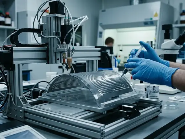
Silver Nanoparticle Drops Meeting on a Heated PET Coupon
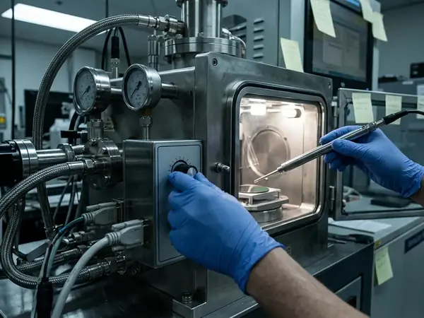
A strobe camera synchronized with a piezoelectric printhead firing pulse at 2 kHz captures the exact moment of drop merging on the observation station. The first silver nanoparticle drop lands on a PET coupon heated to a steady 60°C, spreading briefly before the solvent begins to flash off and the contact line pins to the substrate. Half a millisecond later, the second drop arrives. It strikes the trailing edge of the first, initiating a complex fluid mechanical interaction where the new liquid volume attempts to flow into the rapidly drying bead of its predecessor.
The strobe sequence isolates the formation of the wet bead before solvent evaporation locks in the final geometry. We see the second drop merge only partly into the first. The fluid lacks the time and mobility to level completely across the gap, leaving a distinct inward curve at the intersection. This visible scallop at the merge point represents a localized narrowing of the printed line. The wet bead eventually dries, freezing this scalloped edge into the solid metal trace.
Later in the metrology sequence, a four-point-probe reading flags that exact same segment as a resistance outlier. The physical narrowing observed under the strobe camera translates directly into an electrical bottleneck. The current crowding at this microscopic scallop generates a measurable spike in local sheet resistance, compromising the performance of the entire interconnect.
This single station moment highlights the delicate balance required in conductive inkjet deposition. Controlling the final printed trace quality requires precise manipulation of four primary process levers: drop spacing, solvent evaporation rate, substrate temperature, and particle loading. Adjusting any one of these variables alters the fluid dynamics of the merging drops, shifting the outcome from a smooth, continuous conductor to a series of disconnected, high-resistance islands.
What Drop Spacing and Particle Loading Were Asked to Explain
The team focused on along-trace resistance variation to capture local defects that bulk conductivity masks. A single bulk conductivity number derived from a large printed pad provides a false sense of security. It averages out the microscopic variations, hiding the severe local necking and scalloping that actually drive downstream reliability failures in narrow interconnects.
To relate drop spacing, solvent evaporation rate, substrate temperature, and particle loading to line morphology and electrical performance, the morphological targets were measured at 10-micron intervals along a 50-mm trace. This high-resolution spatial mapping forces a direct confrontation with the realities of inkjet deposition. The morphological targets are defined specifically as drop coalescence completeness and line-edge roughness. A trace might exhibit excellent bulk conductivity while simultaneously suffering from severe line-edge roughness that renders it useless for high-frequency signal transmission or high-current power delivery.
Hidden Bottleneck Risks: High-resolution spatial mapping exposes the localized defects that standard bulk measurements conceal, preventing unexpected field failures in narrow printed interconnects.
The electrical targets prioritize along-trace resistance variation. By measuring the resistance of discrete segments along the 50-mm path, the true electrical penalty of incomplete coalescence becomes apparent. Yield loss and downstream reliability risk emerge as direct consequences of these measurable print artifacts. A scalloped edge is a mechanical stress concentrator and a thermal hotspot, creating a guaranteed failure point under operational load.
How Drop Pitch, Chuck Temperature, and Ink Loading Were Varied
The experimental design executed a factorial-style sweep of drop pitch relative to landed drop diameter, chuck temperature relative to the ink’s solvent volatility, and solids loading of the metal-nanoparticle ink. The substrate was held flat as a polymer film on a vacuum chuck to ensure uniform thermal transfer. Drop pitch was swept from 20 to 60 microns, exploring the entire regime from heavy overlap to isolated droplets. Chuck temperature varied from 30°C to 80°C, modulating the evaporation rate and the resulting fluid leveling time. Solids loading was maintained between 20 wt% and 40 wt%, altering the viscosity and yield stress of the jetted fluid.
The team initially considered varying solvent types mid-run to test evaporation rates. They rejected this approach to isolate chuck temperature as the primary driver, keeping the ink chemistry constant throughout the factorial sweep. Evaporation rate is treated as a coupled outcome of solvent choice and chuck temperature. These specific boundary conditions apply strictly to inkjet-printed nanoparticle traces on heated polymer substrates and do not extend to gravure, aerosol jetting, or sintered bulk metal processes.
The metrology chain operates in strict process language. Optical line-width and edge-waviness inspection occurs immediately after drying. This is followed by four-point-probe or kelvin resistance measurements along the exact same segments. Achieving spatial register alignment between optical edge-waviness and four-point-probe segment resistance ensures that morphology and electrical data share a precise coordinate system. A specific physical neck identified in the optical inspection can be matched to its exact electrical penalty in the resistance data.
Incomplete Coalescence as the Origin of Line-Edge Roughness
A drop pitch that is too large leaves cusps and scallops along the printed line. The drops land too far apart to merge fully before the solvent evaporates, resulting in a series of connected circles rather than a straight-edged trace. Conversely, a pitch that is too small produces bulging, satellite merge, and coffee-ring pile-up at the contact line. The excess fluid volume has nowhere to go, pushing outward and creating irregular, wavy edges.
The scallop-to-bulge transition mapping at the contact line reveals the precise balance required for optimal morphology. Solvent evaporation rate and chuck temperature dictate the time window in which neighboring beads can still flow and level before a skin forms. At 50°C, the leveling time window spans approximately 1.5 to 3 seconds before skin formation. If the drops do not fully coalesce within this brief window, the resulting trace will exhibit severe line-edge roughness.
Particle loading acts as a critical viscosity and yield-stress control. Higher loading slows leveling and can freeze a ragged edge in place before the fluid has a chance to smooth out. The increased concentration of nanoparticles creates a higher yield stress, requiring more energy for the fluid to flow. Lower loading can overspread and thin the conductor, leading to a wider, shallower trace with insufficient cross-sectional area for reliable electrical performance. Researchers mapped the transition from scalloped edges to bulging by adjusting particle loading to control the ink's yield stress, effectively tuning the viscosity during the critical leveling window.
From Scalloped Edges to Resistance Variation Along a Trace
Local necking, scallops, and coffee-ring ridges map directly onto cross-section variation. A scallop is a reduction in line width. A coffee-ring ridge is a localized increase in thickness at the edges, often accompanied by a thinning in the center of the trace. These morphological artifacts modulate width and thickness together, driving local sheet-resistance change along the same printed path.
Optical line-width inspection data correlates with four-point-probe resistance readings by aligning the spatial coordinates of both metrology steps. Sheet resistance measured in discrete 2-mm segments along the trace reveals the scatter that bulk measurements hide. The mean conductivity of a well-sintered film can appear excellent, yet the segment-to-segment resistance scatter remains high due to edge roughness.
Segment Scatter Impact: Cross-sectional variations from scalloped edges create localized resistance spikes that degrade signal integrity, even when the overall trace appears highly conductive.
Sintering locks in the as-printed geometry. It removes the organic ligands and fuses the silver nanoparticles, but it does not heal the macroscopic defects created during the printing process. A scalloped edge remains a scalloped edge after sintering. The electrical penalty of that scallop is permanently embedded in the trace. The spatial register alignment confirms that the highest resistance segments correspond exactly to the narrowest physical necks identified during optical inspection.
Yield Loss and Reliability Risk in Rough Printed Interconnects
Edge scallops and necks link directly to electrical test fallout. High-resistance segments cause immediate yield loss during initial quality control. More insidiously, these defects create opens after sintering shrinkage. As the silver nanoparticles fuse and densify, the trace undergoes volumetric shrinkage. A severe neck lacks the material volume to withstand this shrinkage, pulling apart and creating an open circuit.
Electrical test fallout was traced back to specific morphological artifacts by subjecting the printed traces to thermal cycling. The testing protocol involved thermal cycling from -40°C to 85°C over a span of 120 to 150 hours. The team monitored for open circuits specifically at the previously identified necking points. The probe-to-probe disagreement on the same net highlights the localized nature of these failures.
These artifacts carry severe consequences into field use. Current crowding at necks generates local heating, creating thermal hotspots that accelerate degradation. Furthermore, the scalloped edges act as mechanical stress concentrators under flex or thermal cycling of polymer-backed traces. The coefficient of thermal expansion mismatch between the silver trace and the PET substrate places immense stress on the narrowest points of the interconnect, leading to fatigue cracking and eventual failure.
Primary Literature and Standards Cited for Inkjet Trace Quality
The methodology relies on established printed electronics metrology to ensure rigorous evaluation of trace quality. The IEC 62899 series (2016–2022) provides the foundational framework for printed electronics, defining the standard procedures for measuring line morphology, edge waviness, and electrical performance. These standards ensure that the optical inspection and four-point-probe measurements follow recognized protocols for flexible substrates.
The IPC-2292 (2018) guidelines dictate the design rules for printed electronics on flexible substrates. This standard informs the acceptable tolerances for line-edge roughness and along-trace resistance variation, providing the baseline for evaluating yield loss and reliability risk. The guidelines establish the critical thresholds where a morphological defect becomes a functional failure.
The foundational fluid dynamics principles are drawn from Soltman and Subramanian's work on inkjet-printed line morphologies and temperature control of the coffee ring effect. This research details the precise mechanisms of drop coalescence, contact line pinning, and solvent evaporation that govern the formation of scalloped edges and bulging. The broader context of functional material deposition aligns with the principles outlined in the review of inkjet printing of functional and structural materials. Standards and foundational literature were selected specifically because they address temperature-controlled coffee ring effects and flexible substrate design rules.
A Copyable Process Window for a Silver Nanoparticle Line on PET
Print a single silver-nanoparticle interconnect on PET using this explicit station setup to establish a reliable process window. Begin by jetting an isolated drop onto the unheated PET substrate. Allow the drop to freeze-dry completely, then measure the landed diameter using the optical inspection system. For this specific silver nanoparticle ink on PET, the landed diameter measures 45 microns.
Set the drop pitch to a 25% to 35% overlap band relative to that 45-micron landed diameter. This specific overlap ensures that the wet beads merge before the solvent skin forms, preventing the formation of isolated cusps. Next, set the chuck temperature to 60°C. This temperature is high enough to pin the contact line rapidly, preventing excessive spreading, yet low enough that neighboring drops still coalesce within the approximately 1.5-to-3-second leveling window.
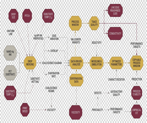
Hold the particle loading steady at 30 wt% to maintain the ink within its printable viscosity window, and do not change the solvent mid-trial. For example, if optical inspection shows scallops on the first coupon printed at 60°C, a second coupon can be printed with the drop pitch reduced by 2 microns. Inspection of that coupon shows whether the narrower pitch cleared the scallops; if the edge instead bulges, the comparison points to a wider pitch or a 5°C increase in chuck temperature.